Warum Patent-de?
Expertenbewertungen, denen Sie vertrauen können
Tauchen Sie ein in detaillierte Bewertungen von Gaming-Fans. Unser Team testet jedes Casino sorgfältig, um sicherzustellen, dass Sie einen echten Überblick über Gameplay, Boni und Kundenservice erhalten.
Exklusive Boni nur für Sie
Schalten Sie spezielle Boni und Werbeaktionen frei, die nur unseren Besuchern zur Verfügung stehen. Wir verhandeln mit Casinos, um Ihnen die besten Angebote zu unterbreiten und Ihr Spielerlebnis von Anfang an zu verbessern.
Sicheres Spielen
Ihre Sicherheit hat für uns oberste Priorität. Wir bieten nur seriöse Casinos an, die lizenziert und reguliert sind, und sorgen so für eine sichere Umgebung, in der Sie beruhigt spielen können.
Benutzerfreundliche Oberfläche
Finden Sie ganz einfach Ihr perfektes Casino-Match. Dank unseres intuitiven Website-Designs können Sie problemlos durch Rezensionen, Bewertungen und Empfehlungen navigieren.
Auf unserer Website finden Sie:
-
Online Casinos mit hoher Gewinnchance
Online Casinos mit hoher Gewinnchance bieten Spielern eine faszinierende Möglichkeit, ihre Gewinne zu maximieren. Diese Casinos zeichnen sich durch Spiele aus, die nicht nur unterhaltsam, sondern auch fair und transparent sind, wodurch sie den Spielern bessere Chancen auf Erfolg bieten. Dank rigoroser Prüfungen und Zertifizierungen durch unabhängige Institutionen können sich Spieler...
-
Beste Bitcoin Casinos
Beste Bitcoin Casinos revolutionieren die Online-Glücksspielwelt mit ihrer Innovation und Sicherheit. Diese Plattformen bieten eine nahtlose und sichere Möglichkeit, Ein- und Auszahlungen mit der digitalen Währung Bitcoin vorzunehmen, wodurch die Privatsphäre und Anonymität der Spieler gewahrt bleibt. Abgesehen von der finanziellen Diskretion profitieren Spieler auch von schnellen Transaktionen, da...
-
Online Casinos mit schneller Auszahlung
Online Casinos mit schneller Auszahlung stehen bei Spielern hoch im Kurs, da sie nicht nur für ihr breites Angebot an Spielen, sondern auch für ihre Effizienz und Zuverlässigkeit bei der Gewinnauszahlung bekannt sind. Diese Casinos verstehen die Bedeutung der Zeit für ihre Nutzer und setzen deshalb auf schnelle und unkomplizierte Auszahlungsverfahren. Dank modernster Zahlungstechnologien können Gewinne oft...
-
Online Casinos mit Echtgeld
Online Casinos mit Echtgeld bieten Spielern die aufregende Möglichkeit, echtes Geld zu gewinnen, während sie ihre Lieblingsspiele von zu Hause aus oder unterwegs genießen. Diese Plattformen verbinden den Nervenkitzel und die Atmosphäre traditioneller Casinos mit der Bequemlichkeit und Zugänglichkeit des Internets. Spieler können aus einer Vielzahl von Spielen wählen, darunter Spielautomaten, Blackjack, Roulette, Poker und...
-
Ausländische Online Casinos
Ausländische Online Casinos eröffnen Spielern weltweit die Möglichkeit, eine breite Palette an Glücksspielen zu entdecken, die möglicherweise in ihren eigenen Ländern nicht verfügbar sind. Diese internationalen Plattformen bieten eine einzigartige Mischung aus Spielen, Boni und Spielkulturen, die von den besten Praktiken und Innovationen aus verschiedenen Teilen der Welt inspiriert sind. Spieler können...
-
Willkommensbonus für Schweizer
Der Willkommensbonus in Online Casinos ist eines der verlockendsten Angebote, die neue Spieler beim Eintritt in die Welt des Online-Glücksspiels erwarten. Diese Boni sind speziell darauf ausgerichtet, Neukunden einen besonders attraktiven Start zu ermöglichen, indem sie ihnen zusätzliches Spielguthaben oder Freispiele zur Verfügung stellen. Der Zweck eines solchen Bonus ist...
-
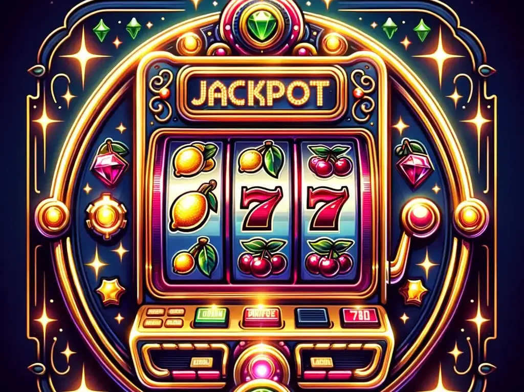
Besten Spielautomaten
Die besten Spielautomaten in Online Casinos zeichnen sich durch ihre Unterhaltungswert, innovative Spielfeatures und die Chance auf hohe Gewinne aus. Hier sind einige der beliebtesten und hoch angesehenen Spielautomaten, die sowohl bei Anfängern als auch bei erfahrenen Spielern großen Anklang finden....